

Huawei unveils ambitious chip roadmap
Firm targets near-frontier transistor density by 2031
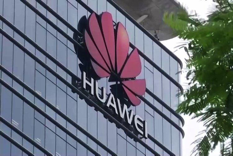
Huawei announced an ambitious chip roadmap aiming to achieve transistor densities equivalent to a 1.4‑nanometre process by 2031, advancing a strategy the company calls the Tau Scaling Law to boost performance without relying solely on ever‑smaller nodes. Huawei said the approach prioritizes reducing signal and data travel time across chips and systems and will use a related architecture, LogicFolding, in its next Kirin series due in late 2026 to shorten on‑chip wiring and raise effective density and speed. The company provided no independent performance verification alongside the claim.
The target is notable because 1.4 nm is projected to be near the global frontier for advanced chipmaking by the end of the decade, yet China faces limits in reaching that frontier via conventional manufacturing after U.S. export controls curtailed access to leading lithography equipment and other critical semiconductor technologies. Huawei framed Tau Scaling as a way to mitigate those constraints by emphasising system‑level innovation, design efficiency and tighter domestic supply‑chain integration rather than sole dependence on cutting‑edge fabrication tools.
Analysts said the plan fits broader national efforts to build semiconductor self‑reliance in China, combining alternative architectures, software optimisation and partnerships with local foundries and research institutions to narrow capability gaps. Observers caution, however, that significant obstacles remain: advanced lithography and production capacity still lag global leaders, and Huawei did not publish third‑party benchmarks to substantiate the 2031 projection. The company’s heavy R&D spending and move toward domestic ecosystems increase the chance of incremental gains, but experts stressed that whether architectural and system innovations can fully substitute for access to the most advanced manufacturing remains uncertain.
The announcement highlights intensifying tech competition between China and the United States across AI, telecoms and high‑performance computing. Huawei and other Chinese firms say alternative design paradigms could preserve performance growth under sanctions, while Western observers view the effort as a test of how far architecture and integration can compensate for restricted access to top‑tier fabrication tools.